
/ 01 全文速览 /
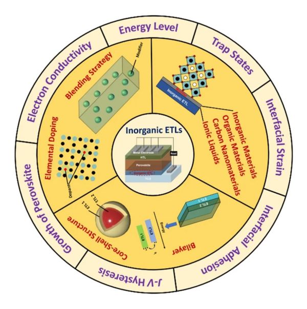
无机电子传输材料因其物理化学稳定性高、制备工艺简单、光伏性能优异以及成本低廉等优势,成为构建高效、稳定的钙钛矿太阳能电池的核心材料之一。然而,此类材料载流子输运能力限制、高缺陷态密度及其与钙钛矿层的能级不匹配等问题极大影响了器件的性能与稳定性。基于此,学院潘军教授团队在Nano Energy期刊发表了题为“Recent progress in improving strategies of inorganic electron transport layers for perovskite solar cells”的综述。综述总结了钙钛矿太阳能电池无机电子传输层的最新研究进展,详细阐述了当前无机电子传输层的优化策略,分析了常用改性策略的优势与不足,并对未来以实现钙钛矿太阳能电池商业化为目标的研究方向提出了展望。
/ 02 研究背景 /
/ 03 本文亮点 /
/ 04 图文解析 /
1. 无机电子传输层的不足
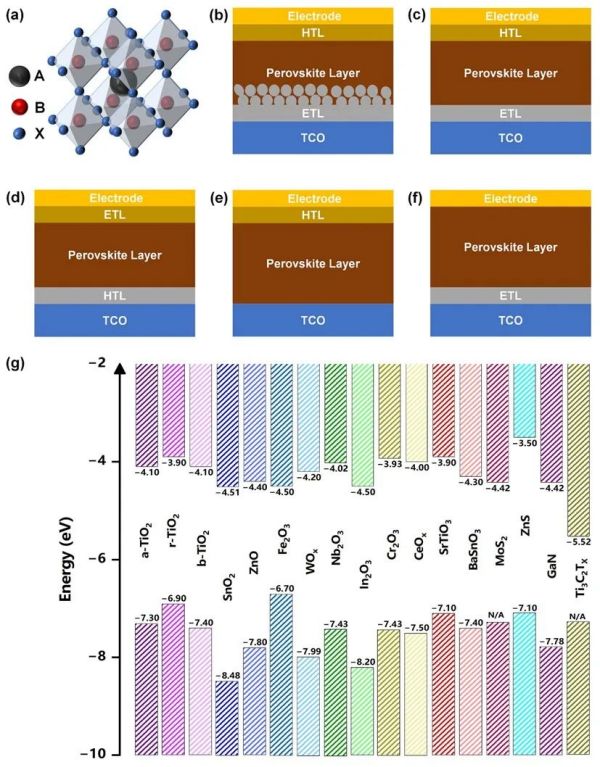
Figure 1. (a) Typical structure of ABX3 perovskite materials. The PSCs based on (b) regular mesoporous, (c) regular planar, (d) inverted planar, (e) ETL-free, and (f) HTL-free structures. (g) The energy levels of various inorganic ETLs. Reproduced with permission.
2. 优化措施
2.1. 元素掺杂 2.1.1. 氧空位有利还是有害?
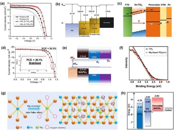
Figure 2. (a) J-V curves of Zr4+-doped compact TiO2 in forward scan and reverse scan direction. (b) Energy levels diagram of SnO2 ETLs with and without Zr4+ doping. (c) Energy levels diagram of PSCs based on Sn4+-doped TiO2. Reproduced with permission. (d) J-V curves of Nb5+-doped SnO2 in forward scan and reverse scan direction. Reproduced with permission. (e) Energy band diagram of the PSCs based on SnO2 and Sb3+-doped SnO2. (f) Valence band spectra of the ETL films with and without the Mg2+ doping. Reproduced with permission. (g) Diagrammatic sketch for self-doping, charge recombination and transport influenced by Mg. (h) Energy level alignment of SnO2 with and without Mg. Reproduced with permission.
2.1.2. 电子传输层掺杂只对电子传输层起作用吗?
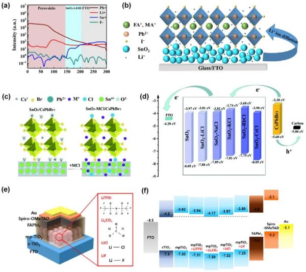
Figure 3. (a) ToF-SIMS depth profile of the perovskite/Li+-doped SnO2/FTO/glass. (b) Schematic illustration of Li+ ions diffusion. Reproduced with permission. (c) Schematic diagram of passivation between CsPbBr3 and the SnO2-MCl ETL. (d) Band alignment diagram of the PSC with SnO2 and SnO2-MCl ETLs. (e) Schematic diagram of PSCs with various Li-salt-doped mp-TiO2. (f) Energy band diagram for pristine mp-TiO2 and various Li-salt-doped mp-TiO2. Reproduced with permission.
2.2. 界面修饰 2.2.1. 界面应力释放助力高稳定性器件 界面修饰策略除了能调整电子传输层的界面能级结构、钝化界面缺陷外,选用合适的修饰材料还可以释放界面应力,从而极大提高钙钛矿太阳能电池的稳定性。此外,不同于WS2等与钙钛矿和电子传输层弱连接的材料,硅烷自组装分子不仅能充当钙钛矿吸光层的“枕头”,还可以极大地提升界面附着力。
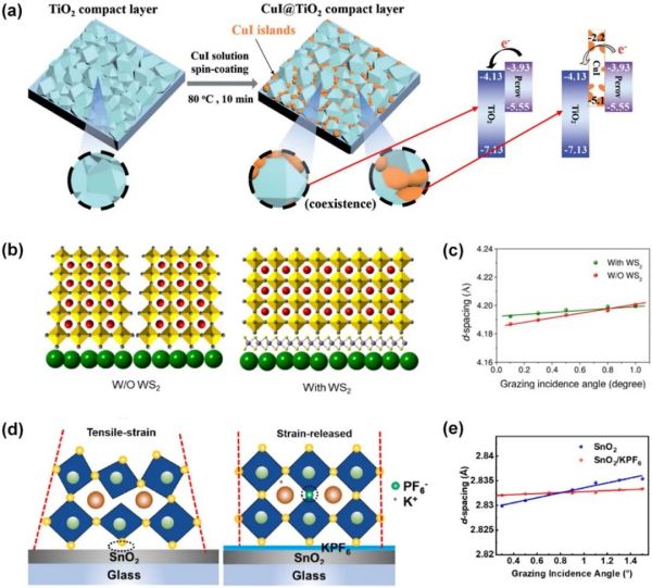
Figure 4. (a) Schematic illustration of the formation of CuI islands on TiO2 compact layer and the energy band structure of CuI@TiO2. (b) Schematic illustration of residual stress distribution in perovskite layer before and after WS2 modification. (c) CsPbBr3 (110) plane as a function of incidence angle. (d) Schematic illustration of residual stress distribution in perovskite layer before and after KPF6 modification. (e) Rb0.05(FA0.95MA0.05)0.95PbI2.85Br0.15 (211) plane as a function of incidence angle. Reproduced with permission.
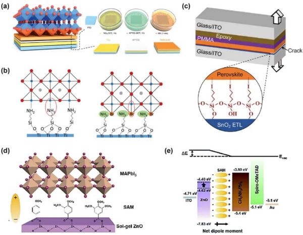
Figure 5. (a) Schematic of fabrication process for TiO2 and PASCA-Br layers. (b) Protonated amino terminals (R-NH3Br) modified interface. (c) Schematic illustration of the I-SAM between SnO2 and perovskite. (d) Schematic illustration of the modified interface by MBA, DMBA, or TMBA. (e) Corresponding energy band diagram of each layer. Reproduced with permission.
2.2.1. 富勒烯及其衍生物的物理吸附还是化学吸附更胜一筹? 尽管物理吸附在无机电子传输层上的富勒烯及其衍生物能改善钙钛矿太阳能电池的效率,但是由于其与电子传输层结合力往往很弱,在沉积钙钛矿层时可能导致其被钙钛矿前驱体移除。因此化学吸附的富勒烯衍生物在提升钙钛矿太阳能电池的稳定性以及效率方面显得更加有效。
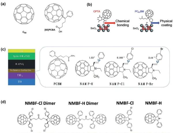
Figure 7. (a) Chemical structure of C60 and PCBA. Reproduced with permission. (b) Schematic illustrations of chemical bond formation between the SnO2 surface and CPTA through an esterification reaction and physical adhesion between the SnO2 surface and PCBM. (c) Schematic structure of the fabricated PSCs and molecular structure of NAMF-H, NAMF-Cl, NAMF-Br and PCBM. (d) Chemical structures of fullerene monomers and dimers. Reproduced with permission.
2.3. 组合策略 2.3.1. 双电子传输层
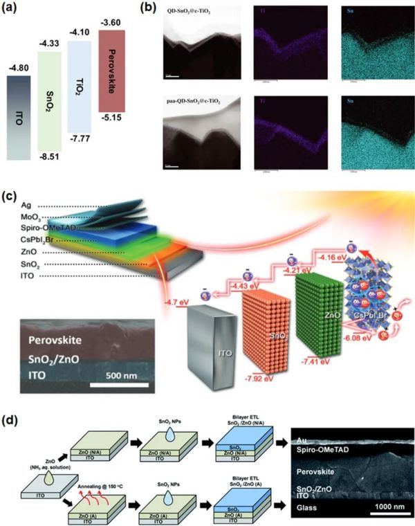
Figure 8. (a) Energy diagram of the layers in the PSC device. Reproduced with permission. (b) Cross-sectional TEM images of QD-SnO2@c-TiO2 and EDS elemental analysis of Ti and Sn for both QD-SnO2@c-TiO2. (c) Device architecture of the all-inorganic CsPbI2Br PSC, the corresponding energy diagrams, and cross-section SEM image of CsPbI2Br perovskite film on SnO2/ZnO. (d) Schematic illustration of the preparation of the two types of planar devices of PSCs and cross-sectional SEM image for the representative device. Reproduced with permission.
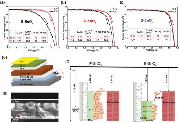
Figure 9. (a-c) J-V characteristics of champion devices with different SnO2 layers in reverse and forward scan. Reproduced with permission. (d) Schematic view of the device structure. (e) Corresponding cross-sectional SEM image of the device. (f) Schematic diagram of the electron extraction process for both types of ETL and energy level diagram. Reproduced with permission.
2.3.2. 核壳结构电子传输层
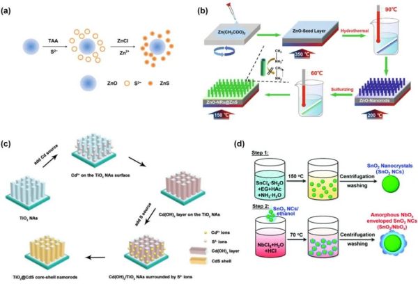
Figure 10. (a) Schematic illustration of the ZnO/ZnS nanoparticles formation mechanism. Reproduced with permission. (b) Fabrication Scheme for the vertically aligned ZnO-NRs and ZnO-NRs@ZnS. (c) The mechanisms of the synthetic of the TiO2@CdS core-shell NAs. (d) Synthetic process of SnO2 and “enveloped” SnO2 NCs. Reproduced with permission.
/ 05 总结与展望 /
/ 06 通讯作者介绍 /

潘军(通讯作者):
浙江工业大学材料科学与工程学院教授,博士生导师,现任材料学院先进材料研究中心副主任,浙江省领军型创新团队核心成员,主持和参与国家及省部级项目6项,获国家海外高层次人才青年项目、浙江省“千人计划”创新长期项目资助。曾于2010年至2019年在阿卜杜拉国王科技大学从事博士后研究和研究科学家工作。主要从事半导体纳米晶的精准合成及其光电器件应用研究,相关成果在Adv. Mater.、J. Am. Chem. Soc.、Angew. Chem.等期刊发表学术论文60余篇,授权国际和国内专利各4项。
http://www.homepage.zjut.edu.cn/pj/
何青泉(通讯作者):
浙江工业大学材料科学与工程学院教授,硕士生导师,博士毕业于上海交通大学。2016年至2020年先后在美国南达科他州立大学和佛罗里达州立大学从事博士后研究。主要研究方向为钙钛矿太阳能电池、量子点光电材料与器件、低维类钙钛矿发光材料等;致力于应用表面改性技术攻克钙钛矿光电材料与太阳能电池器件的效率与稳定性难题,并推动部分成果的产业化进程。在Angew. Chem、Sci. Adv.和Nat. Commun.等期刊上发表学术论文50余篇,H因子29。